This subsection explores the basic principles of a bus and continues to look at some standard implementations, including their timing characteristics.
Example
In our SoC in the lab. this is done in the framestore SRAM interface, although the timing there is known and input data are resynchronised within the interface.
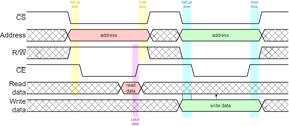
The example above is not the only protocol for bus timing. Another common approach uses an enable (CE) and a direction signal to specify the operation.
Although the data is shown here as unidirectional, off chip buses typically use bidirectional data signals so must be either reading or writing when active. This is due to pin restriction on the package (and wiring on the PCB).
On chip buses are limited by distance but not (particularly) restricted by width because there is a considerable wiring resource on a chip. However on-chip signals are now ‘universally’ unidirectional so that electrical buffers can be inserted along the wire to keep switching edge speed reasonably rapid.


Let's elaborate on that point.
A simple model of ‘load’ on a gate estimates a ‘lumped†’ capacitance. 200 μm of wire will have twice the capacitance of 100 μm. Assuming the same driver, the edge time on the longer wire will be correspondingly greater; thus the signal delay will be greater.
Possible solutions:
However the wires also have resistance which slows down the edge more at greater distances from the driver. The first solution is therefore not as effective as might be though at driving longer wires.
The load can be decreased by ‘cutting’ the wire and inserting buffers (amplifiers) at intervals. These also insert delay but keep the edges fast.
Buffers have an input and an output so the wires, necessarily, are
unidirectional.
The term “buffer” as applied here refers purely to an electrical amplifier. “Buffer” is also used to refer to, for example, latches which hold data and are thus part of the logic. Beware of potential confusion!
†I.e. all the capacitive load is in a single place. In practice it is distributed along the length of the wire which, itself, is resistive: thus the model can be somewhat more complicated.
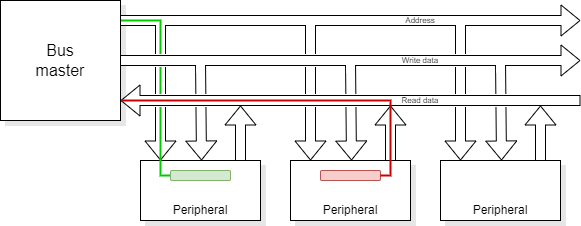
Simple buses are often ‘single-master’, i.e. there is only one initiator which commands all transactions. More complex systems may have ‘multi-master’ buses where the right to initiate a transaction is transferred; this typically requires some form of arbitration.
A simple multi-master example might be a CPU with DMA support. Here the CPU might act both as default bus master and arbiter, with the DMAC requesting (and being granted) bus cycles. More complex systems may have more equality and an external arbiter.
Although often still referred to as ‘buses’ many SoCs have multiple, parallel communications channels and their ‘bus’ structure is more akin to a Network-on-Chip (NoC). AXI systems (q.v.) have this sort of characteristic. This form of connection is probably better described as a “switched fabric” than a ‘bus’ although the shorter term is still in common use!
AMBA is an open standard (or set of standards) which have become a de facto standard for on chip interconnect. The standards specify the list of signals used in the interconnection and their timing relationship on a cycle-by-cycle basis. It was first introduced by ARM Ltd. in the 1990s and has been developed continually, since.
AMBA comes in several ‘flavours’, including:
which are used here as examples.
The different standards represent different points in the complexity/performance spectrum. Thus APB is simple but slow – intended for communication with many, low-bandwidth peripheral devices. Because peripheral accesses are rare in comparison with memory reads and writes a few slow cycles do not impact overall performance significantly.
AXI is better suited for high-bandwidth communications. An example would be the data bus from a memory controller which was frequently used. It allows bursts of data to be communicated and several outstanding transactions at any time, so operations can be pipelined. The price is a significant increase in complexity at the interfaces.
AMBA is not the only standard in use for on-chip interconnect. Open Core Protocol (OCP) is an attempt to provide a standardised ‘socket’ for plugging together Intellectual Property (IP) blocks to make a chip. It is now supported by the Accellera Systems initiative; see: http://www.ocpip.org for further details.
The Wishbone Bus is another open source bus, used in many OpenCores projects. Here is the latest specification (at time of writing).
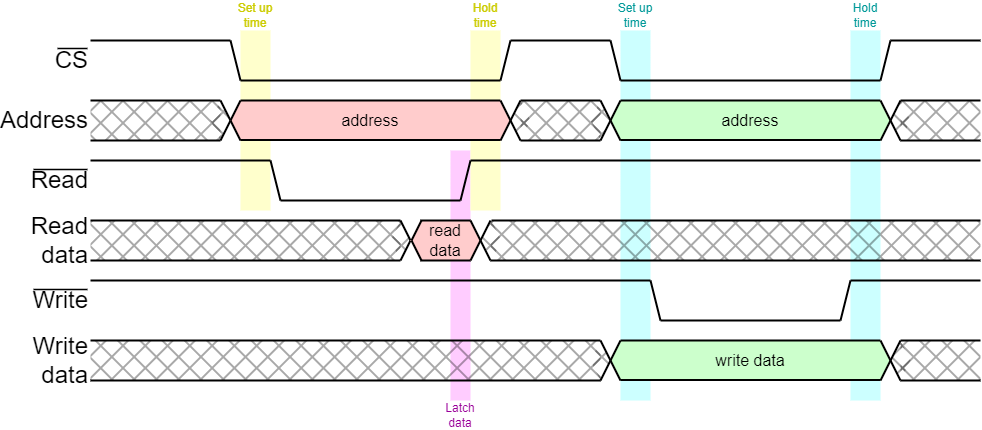
APB is basically a straightforward microprocessor bus. The bus master puts out a command, address and (possibly) write data or (possibly) latches read data at the end of the cycle.
APB is a simple bus model where commands and addresses – and possibly write data – are output at the beginning of the bus cycle and any read data is read at the end of the cycle. Thus there needs to be adequate time for a ‘round trip’ within the bus cycle.
The first APB spec. performed every transfer unconditionally in two clock cycles. This was subsequently extended so that slow peripherals can insert extra ‘wait’ states to extend the cycle time if they cannot respond quickly enough. Wait states may be acceptable when communicating with peripheral devices because such accesses are infrequent so the penalty is small.
Another extension was an error signal, so the failure (abort) of a bus cycle can be signalled.
When a bus master is designed it is not always determined what will be on the other end of it.
A bus transaction may be successful – or it may fail for a number of reasons:
Segmentation faults are typically ‘fatal’ for a thread; page faults require some rearrangement of the memory map.
Many of these are detected by a Memory Management Unit (MMU) before reaching the bus. However, some requests are not, or cannot be, trapped there and cause a bus cycle.
A bus will typically have a status signal returned from the slave device which indicates whether the cycle has completed successfully or if there was a bus error and it has been aborted.
A peripheral I/O device may have only a small number of registers (say 16) but be allocated a ‘page’ (say 1 KiB) of the memory map. It could indicate if an access was apparently to that device but not to one of its valid registers. Alternatively, it could indicate an attempt to write to a read-only register.
This cannot be done by a typical MMU which will not resolve translations to individual words, only pages.
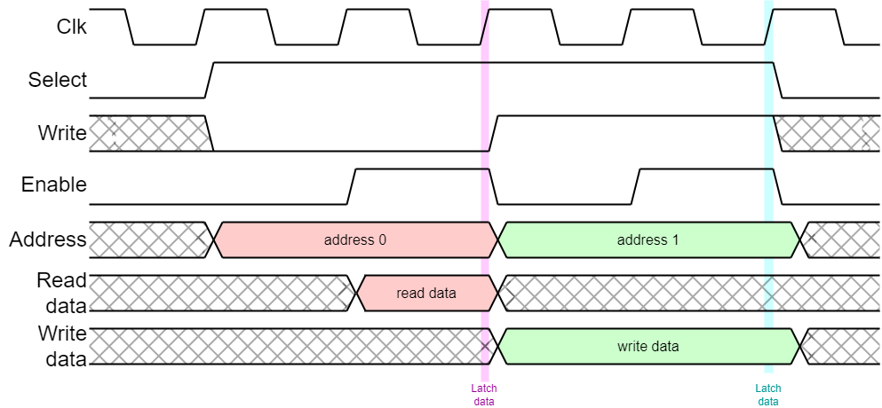
AHB is a pipelined bus intended to perform one transfer per clock cycle.
AHB increases performance by pipelining. For example, in a read operation it outputs an address and status asking for the read on a rising clock edge. This is decoded and selects the appropriate slave device.
On the next active clock edge the slave is expected to latch the address and start the read. At this point the bus master can start the next cycle.
On the next active clock edge the master must:
This sequencing allows faster bus throughput but causes certain difficulties when things don't go smoothly.
Like instructions in a processor, keeping communications cycles in order makes recovery from the exception (abort) very much simpler.
AHB operation is pipelined, so that as one set of data is transferred the subsequent address can be sent.
A different philosophy:
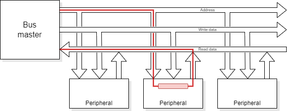
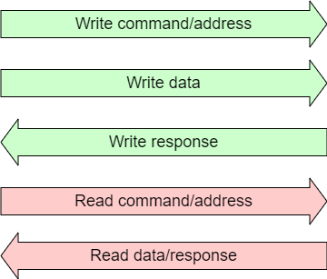
Write command/address Write data Write response Read command/address Read data/responseAXI is more like a network (or ‘switched fabric’) than a bus. Transactions can be initiated from various units and will arrive at various destinations. In between they may be arbitrated and multiplexed as desired. The packet IDs allow steering so that the correct response is returned to the correct initiator. AXI is quite widely supported and has gone through several generations: at time of writing the most recent was AXI4.
Data can be pipelined to reduce the distance travelled per clock cycle and, consequently, allow faster clocking and higher throughput.
Protocol
This is faster than, for example, a handshake which might go through several states and take (no fewer than) four clock cycles to complete one operation.
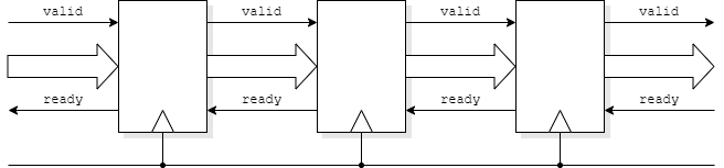
Data can move on every cycle if a pipeline stage can accept and pass on data simultaneously. They may work on this assumption, providing they can cope with buffering data even if the output is denied.
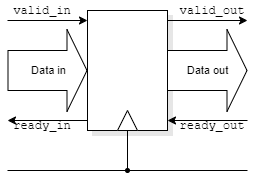
Consider a synchronous AXI pipeline stage.
The intention is to pass data on every clock cycle.
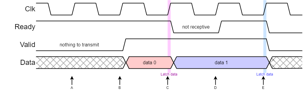
Data moves across an interface if both valid and ready are active.
If you indicate (upstream) you are willing to accept data (ready) that is a commitment.
There is not time to propagate a control signal throughout the pipe!
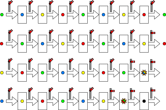
If a blockage propagates backwards at one stage per clock data in adjacent latches will collide – some data will be lost.
(Figures will ‘pop out’.)
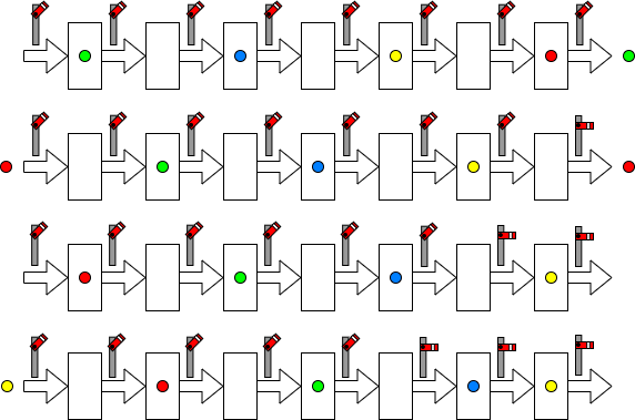
With sparser occupancy data can stop safely; however throughput is reduced.
This is much like the traffic on a road.
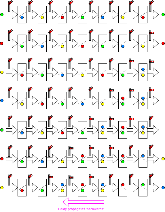
With extra buffering it is possible to achieve ‘full’ throughput and still stall the pipe locally.
The disadvantage is the overhead in extra latches.
Note that in some pipelines there will be buffering implicit in the
architecture to ‘even out’ such flow irregularities.
Examples could include network routers storing and forwarding
packets.
Back/up to Interconnection.
Forwards to complex interconnection.