Simple example:
This is an ARM-based microcontroller/SoC we formerly used in the laboratories. It uses:
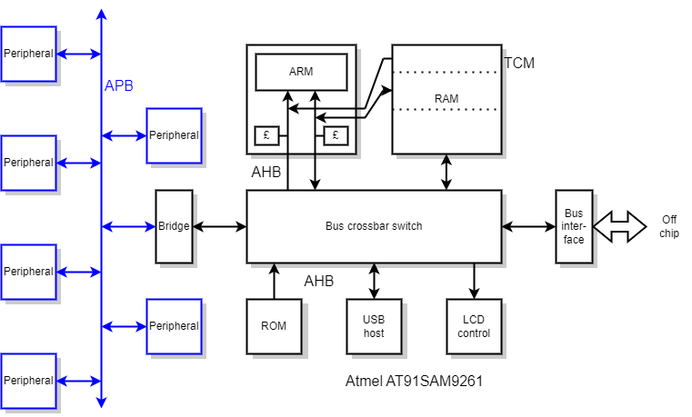
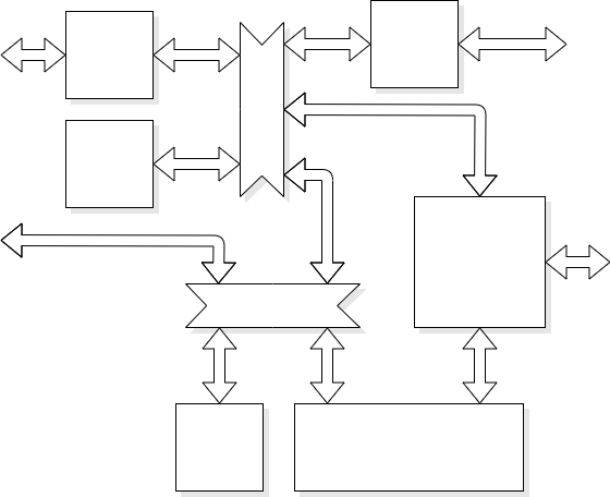
The example given here is the Atmel AT91SAM9261 ARM-based microcontroller. The view shows the interconnection structure around the processor.
The processor masters two buses (instruction and data) which are fed into a bus switch matrix. Other devices can also be bus masters as the USB host interface, the LCD controller and the APB bridge all have DMA capability.
Dependent on the matrix are:
The crossbar switch allows parallel operations so different masters can have access to different slave devices simultaneously. Clashes have to resolved by inserting wait states.
Bus occupancy can be reduced because the processor has:
Tightly Coupled Memory (TCM) maps fast SRAM to specific addresses. (This device has ten individually switched 16 KiB blocks.) This can allow parallel instruction and data access and still leave the I/O buses free for DMA.
TCM is sometimes preferred over cache in microcontroller applications because its timing behaviour is easy to predict. Cache accesses may be faster on average (as the hit rate may be better optimised) but predictability means that a worst case response can be guaranteed – important in some real-time applications.
The APB hosts numerous lower performance peripherals. It may be run at a lower clock speed than the AHBs as a power saving measure.
A bus bridge is simple a means of converting from one protocol to another. Usually a bridge is a slave on one bus and a master of another, although bidirectionality is possible.
When a bus structure becomes sufficiently complicated it can be an advantage to allow transactions to complete out-of-order.
This gives decreased latency for some (urgent) operations at the expense of greater complexity, especially at the master where dependencies between reordered transactions may have to be resolved.
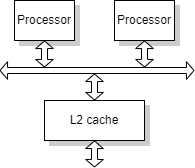
Current generation CMPs typically share a bus to a level-2 cache. This is satisfactory for a small number of processor cores but as the number increases the pressure on this bus increases too. Such designs will not scale well. More elaborate – sometimes hierarchical – bus structures are evolving, although these exacerbate problems with maintaining cache coherency.
Another bus descends to the next level of memory hierarchy.
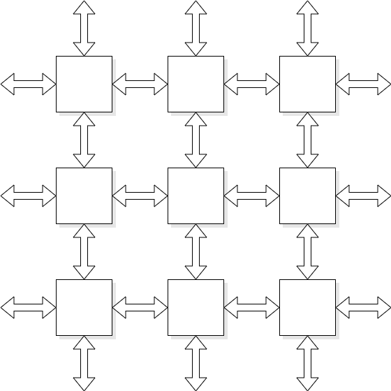
With integration levels increasing, simple bus structures become inadequate.
Starting to develop networks on chip.
There broadly fall into two categories:
A communications mechanism which sends each part (‘packet’) of a correspondence individually. Potentially, unrelated packets may interleave on the same route and/or packets from one session may take different routes.
A communications mechanism which sets up a ‘permanent’ link (for the duration of the communications) dedicated between corresponding units.
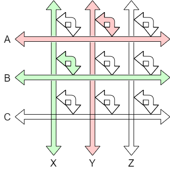
A “crossbar” switch is a many-to-many switch, capable of
supporting multiple simultaneous connections simultaneously —
naturally subject to the constraint that each individual input or
output can only have one correspondent at a time.
They are sometimes referred to as a “switch matrix”.
For example, in a multi-processor system a bus switch crossbar
can allow different processors simultaneous access to different
resources.
As clock speeds increase and wiring delays become more significant it is difficult to maintain a synchronous clock model across a whole chip. This problem was discussed in the section on timing (q.v.).
However one solution to this problem is to allow different IP blocks to be clocked independently with an arbitrary phase and, possibly, at different frequencies. It is then the job of the interconnection to cross the clock domains. (See also clocking notes.)
This form of interconnection is known as GALS (Globally Asynchronous, Locally Synchronous). GALS frees the SoC designers from a number of timing constraints which makes timing closure much easier. Each block is developed as a synchronous circuit but there is no need for chip-wide skew-free clock distribution.
Another advantage is the ability to run each block at its own ‘best’ frequency with the possibility of consequent power reduction.
There can also be a reduction in power supply noise. In a synchronous circuit logic begins to switch just after each active clock edge. Typically the number of gates switching over time diminishes during the clock period because not all logic paths are the same length. When gates switch they pull charge from the power supply or dump it onto the ground. The demand for charge (a.k.a. “current”) therefore varies periodically setting up a regular AC signal in the (extensive) power wiring. This both acts as a transmitting aerial (especially the wiring into the chip) and may affect other gates' switching. If a whole chip is synchronous then this problem is at its worst; if there are several clocks with different phases (or frequencies) the demand tends to even out, reducing noise problems.
There are also disadvantages to GALS' unsynchronised communication. The biggest is the need for synchronisation of signals when they arrive at their destination. This inherently adds some latency to the signal; more if the reliability is increased by adding longer waits for the resolution of any metastability. Communication is therefore slowed down in some way.
The simplest communication mechanism is synchronous on a one-item-per clock basis; this relies on assumptions that data will always be available and accepted on every cycle.
If data is not available on every cycle a ‘validity’ (or “request”) signal can be used to indicate when data is available.
If the receiver may not always accept data then some sort of flow control must be included. Across a synchronous interface – such as AXI, discussed earlier – this can be another status bit.
With an asynchronous interface various assumptions cannot be made and some form of handshake protocol is needed. This must be subject to synchronisation to the local clock, with a concomitant latency penalty.

A simple method of communication between asynchronous blocks is to synchronise each data request and, subsequently, latch the data from the bus. This results in a moderate latency but quite a low bandwidth because every transmission requires two synchronisations, one for the forward request and another for the reverse acknowledge.
Higher bandwidth can be achieved by buffering several data elements for a single synchronisation. The transmitter ‘owns’ a RAM into which it writes a message. When this is complete it passes the RAM to the receiver. After synchronising with the receiver's clock the data can be read out at full speed. The overall latency is greater but the average bandwidth is also higher. This type of mechanism may be further enhanced (at additional hardware cost) by double buffering so that one RAM is filled whilst the previous one is emptied.
At its most extreme the interconnection may be asynchronous logic which can implement an elastic FIFO between transmitter and receiver. This could be a dual-port RAM which is written and read at different rates – synchronisation is only necessary when the FIFO is almost empty or almost full – or truly clock-free circuits.
This last subsection is something of an aside, in that it is chiefly concerned with systems off chip!
For wider system interconnection it is common to use serial interconnection:
Examples include:
Pin restrictions do not apply to intra-chip connections.
Nevertheless the reduction in wiring is becoming attractive for some SoC applications.
In a serial bus transactions must occur as packets, so that the various signals are time-domain multiplexed onto the medium. Thus it may be that a transmitter sends a packet which contains ‘C’ bits of a command (such as read or write), ‘A’ bits of address (which may be a subsystem and/or a memory address) and ‘D’ bits of data.
Ethernet probably seems familiar to you already. It is a peer-to-peer interconnection medium. Originally all the devices simply shared a common communications medium (the ‘Ether’†) although modern Ethernet is typically packet-switched with point-to-point links.
†It was an intellectual joke: it wasn't historically contemporary!
You are probably more familiar with USB (Universal Serial Bus) as a user than aware of its operation. It is a hierarchical structure where devices (slaves) are polled by the host (master) to allow them to transfer data. Data is communicated across a simplex (one direction at once) differential pair (see opposite) serial line.
Communication is asynchronous so each device has to have a precise clock reference matching the specification.
I2C (Inter-Integrated Circuit) is a Philips invention; to avoid legal complications it is sometimes referred to as Two Wire Interface (TWI) by other manufacturers.
I2C is a fairly slow interconnection, suitable for driving entirely in software with two PIO bits if required. It is typically used as a PCB level interconnection, for example for adding memory to small microcontrollers. However it is a multi-master bus where arbitration for mastery takes place via the same two wires.
Communication is synchronous as one wire is used as data, the other as a clock. However the ‘clock’ – really more a strobe – need not be regular as it may be software driven or paused by the receiving device if it is not ready.
SPI (Serial Peripheral Interface) – originally from Motorola – uses a four-wire (sometimes three-wire) serial interface for peripheral chip communications and I/O expansion. It's purpose is much the same as I2C.
A differential signal is where a single logic state is represented by two digital wires which are always in ‘opposite’ states. Legal states are low/high and high/low.
The state of the signal is interpreted by looking at the difference between the wires, which will either be positive or negative – a binary choice.
Differential signalling is used for noise immunity. If two wires are physically close to each other any induced noise is likely to affect them in a similar way. A single wire compared to an unmoving ‘ground’ signal may have its state altered but the difference should be (largely) preserved. This is known as common-mode rejection.
Up to Interconnection.
Back to buses.
Forwards to CMOS circuits.