The diagrams here describe ‘classic’ planar MOSFETs; here the channel is formed just under the surface of the silicon with the controlling gate built above that surface. This technology has served for half a century through almost incredible scaling in size; it is still in regular use.
However once feature sizes drop below ~22 nm the channel Length is so small that it is difficult ⇒ impossible to turn a transistor made this way ‘off’ and more exotic (expensive) constructions have to be made
More on that, later.
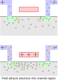
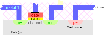
In this n-channel FET, the p-type substrate (or well) will have a contact to ground. If the gate is also at ground (logic '0') then there are reverse-biased diode junctions preventing conduction: the transistor is ‘off’.
If the gate is raised to a positive voltage (logic '1') electrons are attracted which temporarily alters the local silicon properties to have a surfeit of charge carriers (electrons being negative; the diodes ‘disappear’ and the channel conducts – the transistor is ‘on’.
The gate voltage at which the transistor ‘switches’ is known as its threshold voltage (Vth); it can be set by the silicon doping concentrations. For the nMOS transistor this is its voltage above the local ‘low’ voltage.
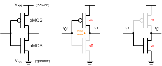
p-channel transistor operation is complementary to this,
operation otherwise being basically the same principle. for a pMOS
transistor Vth is a voltage difference below the
local ‘high’.
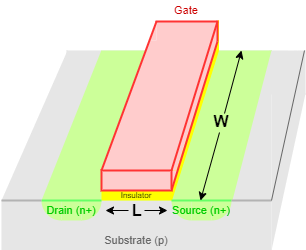
Here we see the basic construction of a MOSFET. Note the gate electrode sits above the channel and is separated from it by a thin layer of ‘oxide’. When a positive voltage is applied to the gate a negative charge is induced in the channel. If the source and drain are n-type material then they need a negative charge in the channel to make the device conduct. This is an n-channel device and the channel will initially be p-type and hence have no negative charge carriers to allow it to conduct.
The opposite is true for p-channel devices (swap ‘n’ and ‘p’). The major geometrical parameters (dimensions) of importance are the length of the channel (L), the width of the channel (W) and the thickness of the gate ‘oxide’ tox.
The channel length is the usual figure quoted for the manufacturing geometry (e.g. “28 nm”).
Or, at least it used to be: some of the newest processes are using numbers more suggestive of marketing than geometry to suggest Dennard scaling is continuing, unabated!
In VLSI design we can control L and W easily using our layout tools. We can also have some control over tox, but this is usually fixed by the CMOS process we wish to use (i.e. by the manufacturer or fabrication house).
The doping levels may also vary which will change the number of free conductors in the ‘off’ state and thus the threshold voltage (Vth) of the transistor. A low-threshold transistor will start to conduct early on as it is switched on and so can be used in a ‘fast’ gate; however it does not turn ‘off’ so well and thus tends to leak charge, thus increasing power dissipation. A high-threshold transistor is slower but better for low-power applications.
The pictured device is an nMOS FET. For a pMOS FET swap ‘N’ and ‘P’ and use a negative gate voltage to repel electrons from the channel to make it conduct.
When drawing layout by hand (a.k.a. ‘polygon pushing’) the diffusion area is drawn both over the gates and the channel (see below); during the ‘implant’ stage(s) of manufacture the drawn areas are exposed whilst the others are masked. This stage occurs after the gates have been manufactured; the transistor gate acts as an additional mask, protecting the silicon below from the ion implant. (The gate will receive some doping in the process but this is harmless or even beneficial.) This is a self-aligning process which ensures accurate relative placement of the gate and channel automatically.
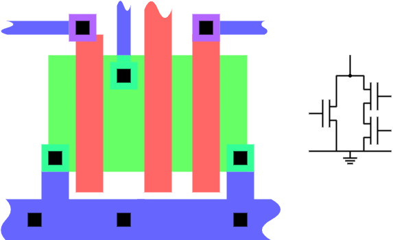
‘Plan’ view where coloured (or textured) polygons represent different vertical layers.
The figure shows a ‘plan view’ of a transistor structure as it might appear in a CAD layout tool. The schematic on the right shows the ‘circuit’ implemented.
The central area is the diffusion area with the (polysilicon) gates striped across it. The small dark squares are the contacts between the layers.
Across the bottom is a metal ground rail which contacts diffusion in two places. This between these points are three transistors, one to the left of the output contact and two, in series to the right. Making structures like this, without intervening metal wires, reduces area and parasitic capacitance.
The inputs arrive on metal (middle one not shown) and contact down onto the gates.
The polysilicon is physically above the substrate (and not connected to it); it is below the metal and could pass under it without contact.
The additional contacts in the metal rail are well contacts which supply charge to the substrate.
There are minimum – and, sometimes, maximum – widths of and clearances between features (e.g. minimum gate length, minimum metal 1 width, minimum overlap of gate at end of diffusion …) which are known as the design rules. These must be observed if the fabricated layout is to work (stand a good chance of working). CAD tools provide an appropriate Design Rule Checker (DRC).
Above the silicon there are several layers of metal wires. Three are shown here; in a modern device there might be ten or more. In reality, especially on higher metal layers, the wires will be proportionally taller (vertically) with respect to their width than shown here. This allows a greater wiring density whilst retaining reasonable conduction paths.
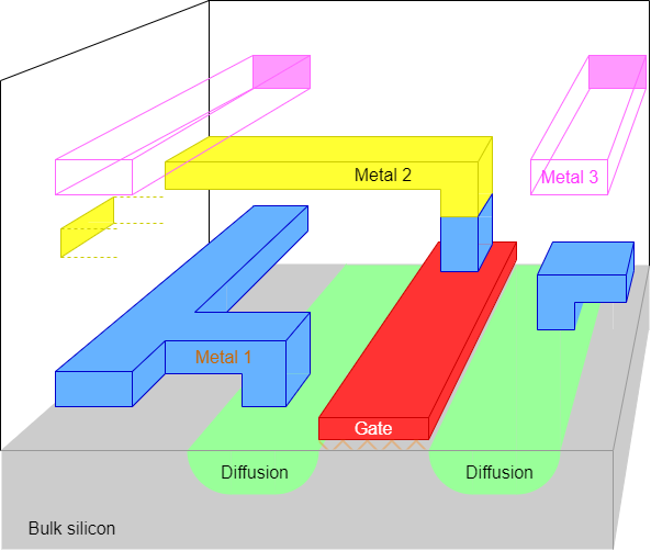
The layers are built up from the silicon in sequence. Inevitably there is some increase in surface roughness so higher level wires may need to be (drawn) wider to ensure good connections. Typically there are also planarisation steps during construction so that subsequent layers have a (reasonably) flat surface to bond to.
The wires were formerly made of aluminium – now typically copper (which is harder to work) because it has lower resistivity.
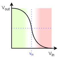
The gate threshold is the input voltage where the gate
output switches.
CMOS is Complementary MOS technology. The pMOS and nMOS transistors complement each other, one being good at pulling outputs high, the other at pulling outputs low.
The simplest demonstration is the inverter.
Sadly, the two types of transistors are not quite complementary. Refer to the sub-section ‘ transistor sizes II’ (next section).
The transfer characteristics shown above are ‘DC characteristics’ i.e. what happens if the input is left indefinitely at a particular voltage. In practice the input would normally be changing ‘rapidly’ and the capacitive load on the output would slow down the output voltage change.
A simplified model of the dynamic behaviour of CMOS switching.
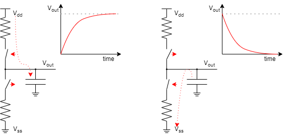
Exponential curves in both cases.
The bigger the load, the slower the output edge. Load is imposed by the inputs of other gates (each transistor gate is a capacitor) and – nowadays dominantly – by the interconnection wiring. Both of these depend on the network fanout; in practice a count of the gates wired to will give some approximation of the scale of the wiring load.
When fanout becomes big, edges can become slow. To alleviate this, use bigger transistors! It is common for a gate library to contain a range of implementations of each logic function (for example {INVd1, INVd2, INVd3, INVd4 …} where the drive strength of the gate can be selected.
There are also disadvantages to bigger gates: more space occupied and more load for whatever is driving them.
To get bigger FETs it is legitimate to place two or more devices in parallel. For example, here are some inverter layouts:
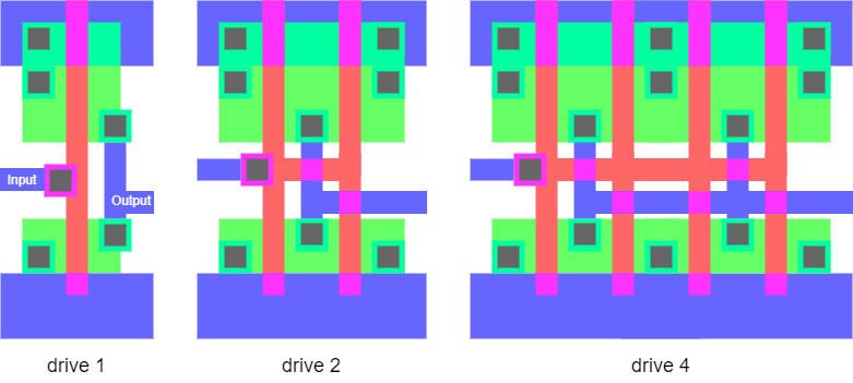
As before, layout is structured to minimise area and parasitic capacitance. The only place where capacitance is not a problem is on the power rails (where additional capacitance helps keep the rail voltage stable).
The majority of (digital) VLSI is built from standard cells. These are implementations of widely used components, largely equivalent to a single gate. There will probably be a selection of complex gates present too.
This process is similar to a compiler mapping a programmer's statements to machine instructions: most microprocessors have roughly the same sort of instruction set but particular details vary.
Each library component will have a counterpart in layout. The layout may be visible to the user although sometimes manufacturers will protect these and only a ‘phantom’ which shows the size and connection points will be seen; in this case the phantoms will be substituted at the foundry. What will be available will be a characterised model of the cell which can be used with appropriate CAD tools to simulate its behaviour with its true capacitive loads, output drive etc.
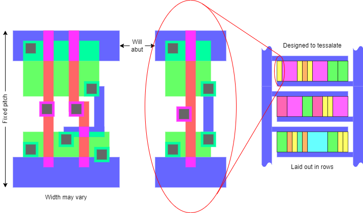
Standard cells will be designed with a fixed height with power rails of a known width in defined places. They will be different widths although it may be the case that these are all multiples of some standard unit (to fit more easily on a ‘grid’).
Cells will already be DRC correct internally and will be DRC correct when abutted; this will usually include when reflected ‘left-right’ and, sometimes also ‘top-bottom’ where power rails may be abutted or even shared.
Layout is typically in rectangular blocks with power fed from (wider) rails at the edges. (Other power rails may be placed on higher metal layers and linked down.) Typically standard cells can be reflected laterally if it makes routeing† easier. Some standard cells may be designed so that their power rails may be overlapped/abutted so that ever alternate rows are ‘upside-down’, thus sharing the conductor and saving some space; this also shares the wells (see figures).
Dummy ‘spacer’ cells will be added to fill in any gaps and may fulfil other functions such as providing well contacts. In modern processes it is likely that (at least initial) layout will add extra spacers to give room for later ‘in-situ’ modifications such as buffer insertion. The keyword here is “utilization”‡ which represents the proportion of the available space which is actually being used.
In an ASIC the available space is the chip area allowed for that particular synthesised block. This may be reversed so that the designer specifies a utilization as a constraint for the layout tools and it claims an appropriate area having estimated the necessary cell area from the design. Higher utilization makes more efficient use of space (reduces cost) but makes it harder to route successfully; a typical starting point might be around 70%, subsequently adjusted in an attempt at optimisation.
A given FPGA has a fixed set of resources so the utilization is based on this. It can be a guide to how much ‘room’ is remaining for design changes or might indicate that you could use a smaller (cheaper!) device. By the time you've completed this module you should have looked at some real FPGA utilization figures.
† Spelled the British way. 🙂
‡ Probably spelled the American way.
The exact mix of cells in a cell library will vary but it can be expected that there will be most or all of the ‘common’ gates such as inverters, AND, NAND, OR, NOR, XOR and XNOR with a range of input counts. These will typically come in a range of drive strengths too.
There will probably be a number of the simpler complex gates (and-or-invert, or-and-invert) because these can often reduce the logic depth (and hence the critical path) of a logic block.
The design as specified needs to be converted into cells which can be laid out on chip. This phase is called ‘technology mapping’. CAD tools convert the circuit specification into cells from a component cell library.
Some latching elements will be present, including a number of D-type flip-flop variants (with/without resets, enables etc.) and probably some transparent latches.
Other cells are less likely but multiplexers (exploiting transmission-gate technology for speed) are not uncommon.

Remember that a single CMOS logic stage has an inverting output {INV, NAND, NOR}. A standard AND gate will typically therefore be a NAND-INV combination, which will be slower although the output inverter gives it good drive strength. However if ‘large’ fan-in gates are present they may be compounds of other structures and non-inverting cells may be preferred.
This second case is because there is a practical limit to the number
of series MOS transistors in any given stack.
In some modern processes standard cells may be available in different pitches, allowing of cells with different effective ‘widths’ (or number of fins: see later lecture) to be interspersed in different rows.
It's another way of cramming more into the space.
Some components would be very inefficient in speed/area/power if made from standard gates and are sufficiently common that they are worth generating differently. The most common examples are memories.
For example there may be a ‘RAM generator’ tool which can be fed parameters (such as the number and size of the words) and will produce a block of layout accordingly. This is facilitated by the regular, tessellating structure of RAM cells.
Memories such as Static RAM (SRAM) and ROM generated this way will be much more compact than a ‘DIY’ approach using D-type flip-flops etc. (Maybe 10× denser or more.)
Similarly, a ‘flat’ netlist may serve for small devices.
For an SoC it may be ‘better’ to layout a device hierarchically.
Modern FPGAs can make extensive use of macrocells, although these have to be designed in at manufacture. Typical examples include:
It is, of course, possible to layout components by hand, lovingly crafting every transistor to exactly the desired dimensions. Of course, in practice this is not economic on an SoC scale.
Hand design may still be done to create standard cells and specialist structures but, except when trying to squeeze the last bit of performance out of a design, higher level structures will be built of pre-prepared cells. Hand composition of standard cells is also possible (to simplify and reduce wiring runs) but is, again, unusual.
One of the major problems with hand-building layout is that it is non-portable. The design rules – the geometrical parameters for the manufacturing process – will differ in each silicon foundry and, within a foundry, change from process to process. Design at a higher abstraction level may lose a small amount of performance but gains portability (and reduces development time).
Hand placement, especially of large components (macrocells) may still be valuable as a ‘hint’ to the place-and-route tools. Perhaps ironically this can help particularly with performance on FPGAs.
Although we are really concerned with digital design it is possible, and sometimes necessary, to build analogue circuits too. An example would be a voltage controlled oscillator used in a PLL clock multiplier. In practice a significant proportion of a SoC will contain analogue components.
When analogue and digital parts are both present on a chip it is known as a ‘mixed signal’ design.
Analogue circuits are usually constructed using the same types of MOSFETs as the digital devices; this keeps manufacturing cost down. Some other devices, especially capacitors may be included. (For example, a capacitor may be formed from the gate of an otherwise unused FET or from interleaving ‘fingers’ of metal wiring.)
Analogue design is a separate – and specialist – skill.
Back/up to CMOS index.
Forwards to gate structures.