CMOS
This ‘chapter’ looks at the commonest – indeed
almost universal – technology for implementing digital
circuits. The chips are not confined to digital logic:
the process can usually (often must!) integrate analogue
components on the same die (this is called “mixed signal”)
but out main interest is in logic gates. This is the Complementary
Metal Oxide Semiconductor process.
The MOSFET
- Metal Oxide Silicon Field Effect Transistor
- Three terminal device
- …Source – source of charge carriers (current)
- Drain – sink for charge carriers (current)
- Gate – potential (voltage) on gate controls current flow
- and a fourth (substrate) which we normally omit from figures
- We use enhancement mode devices
- Normally turned off
- Need to enhance conduction using potential on GATE
- Come in two ‘flavours’ p-channel (pMOS) and n-channel
(nMOS)
- Devices are symmetric
- No physical difference between source and drain –
just labels.
In the VLSI world this primarily refers to
silicon.
FETs rely on (controlled) currents flowing in the semiconductor
material. Pure silicon does not conduct electricity well, but can be
given additional charge carriers by
doping
with atoms with different valences. n-type dopants – which
contribute an extra conduction electron – include phosphorus,
arsenic and antimony; p-type dopants include boron, aluminium and
gallium, which introduce extra ‘holes’ which are the
equivalent positive charge carrier. The reason for this is apparent
in the periodic
table.
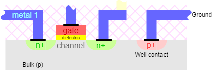
A MOSFET consists of a drain and a source contact with a channel in
between which is doped such that it will not conduct when a potential
is applied between the drain and source. It cannot conduct because it
has no charge carriers of the type produced by the source electrode.
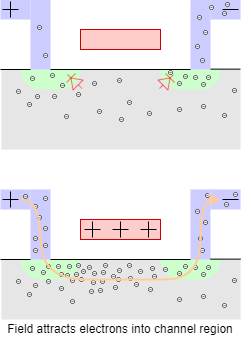
If a suitable potential (voltage) is applied between the gate
electrode and the source then charge is induced in the channel by the
electric field set up across the gate oxide layer. This charge
consists of the same type of carriers as in the source and hence the
device can conduct.
With n-type doping in the source (electron donors) we need to induce a
negative charge in the channel (initially p type material). This gives
an n-channel device. Alternatively we can dope the source with p-type
impurities and produce ‘holes’ which act as positive
charge carriers; then a positive charge need be induced in the
(originally n-type) channel to make it conduct. This is a p-channel
device.
As the device is normally off and a voltage is required on the gate to
make it conduct this type of MOSFET is known as an enhancement
mode device.
Depletion mode devices exist (normally conduct until turned off
by a voltage on the gate) and these can be useful in logic circuits
but not as switching elements. They tend to be mainly used as active
load devices and have some advantages over simple resistor loads.
Note that the substrate (“bulk”) connections are often
omitted from circuit diagrams of logic gates for simplicity. They are
present on the actual devices. If we think of the channel as one plate
of a capacitor with the other being the gate then the substrate
provides the potential reference for the channel plate. It provides
the carriers induced into the channel by the gate potential. Thus in
n-channel devices it is connected to the most negative potential in
the system and in p-channel devices to the most positive potential.

Diode junction
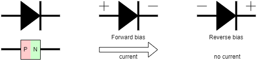
- A semiconductor diode is formed by a junction of P-doped and
N-doped material.
- The ‘ideal’ diode allows current to flow from P to N
but not vice versa.
- A real diode will require some finite forward bias voltage to make
the current flow.
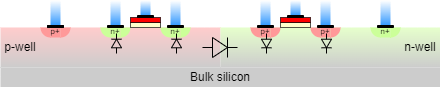
Diode junctions in CMOS
- Not employed directly as an active component.
- Implicit in isolating FET channel when ‘off’
- Implicitly separate ‘wells’ in which transistors are built:
- P-well holds N-channel transistors and is connected to ground.
- N-well holds P-channel transistors and is connected to ‘supply’.
Basic structure of the MOSFET
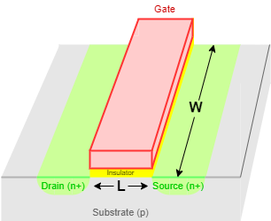
The diagrams here describe ‘classic’ planar
MOSFETs; here the channel is formed just under the surface of
the silicon with the controlling gate built above that surface. This
technology has served for half a century through almost incredible
scaling in size; it is still in regular use.
However once feature sizes drop below ~22 nm the
channel Length is so small that it is
difficult ⇒ impossible to turn a transistor made this
way ‘off’ and more exotic (expensive) constructions have
to be made
More on that, later.
CMOS transistor structure
- Metal – gate (first metal, then polysilicon, now typically
metal again)
- Oxide – insulator (SiO2); these days usually a
‘high-k dielectric’ instead
- Silicon – substrate doped with Boron, Arsenic,
Phosphorus …
- Field – no current flows in the gate; the electric
field causes an
- Effect – which ‘sucks in’ (or ‘drives
away’) electrons to control the
- Transistor
CMOS: links
In this session
Other