
This page delves into some esoteric details. Hopefully it's a bit interesting and shows how the available components (MOSFETs) can be used in different ways; these techniques will normally be confined to the inside of standard cells (e.g. latches) or macrocells (e.g. SRAM) so this is low-level detail.
Transistors not ‘explicitly’ stacked to appropriate power supply.
Transistor as a switch: nMOS transistor passes ‘0’ but poor at passing a ‘1’
pMOS transistors can be employed in a similar way.
Note FETs are symmetrical so a ‘signal’ can pass in either direction.
If the gate on an nMOS transistor is grounded it is not going to be higher voltage than the channel (bulk) thus the transistor is ‘off’. In Verilog terms the far side will be ‘Z’ (high impedance) unless something else is driving it.
If the gate is ‘high’ then the transistor will be ‘on’ provided that it has something to be ‘high’ relative to. Thus it will ‘pass’ a ‘0’ quite happily. It will not ‘pass’ a ‘1’ because, as the output approaches ‘1’ the transistor turns ‘off’ and thus never quite gets there.
On the other hand a pMOS transistor will happily pass a ‘1’ but is not very good at passing a ‘0’.
Sometimes this is adequate on its own: a lot of the time it is not so satisfactory.

An example of n-pass transistors is typically found in SRAM cells. When writing to a cell the word line is ‘high’ and the bit lines are (strongly) driven to opposite states; the inverters are small† so the struggle is unequal and one side of the cell is pulled to (near) ‘0’. The other side is pulled ‘high-ish’. This is enough to ensure the cell is in the desired state and the full voltage swing will be made up (relatively slowly) by the back-to-back inverters.
The inverters are small, the bit lines are big (capacitive) so when reading an analogue amplifier is used to compare the bit lines so a full-rail swing is not required.
nMOS pass transistors are chosen because their transconductance is
better for a given size than pMOS.
†As small as possible to get the most bits in the least area.
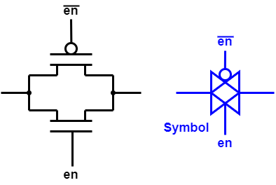
nMOS passes ‘0’ well but ‘1’ badly. pMOS passes ‘1’ well but ‘0’ badly.
Acting together they can make a useful digital switch; one transistor dominates when switching in each direction.
Note that complementary enables are required.
A transmission gate is a switch: it will pass current (thus signals)
in either direction. This is useful but can also cause problems:
without buffering ‘outputs’ may have unwanted effects on
‘inputs’.

Example: a multiplexer can be built using transmission gate switches internally; some standard cells may contain such structures. The example shown may be superior to the same functional cell using CMOS gates, particularly as its output driver is a simple inverter which has the best drive-strength-per-size of any ‘gate’.
This type of structure also scales quite well, e.g to a 4:1 mux.
Whilst once using bidirectional signal wires on-chip was not unusual it is rarely (if ever) expedient in contemporary technology; this is now largely confined to inter-chip connections such as a data bus to external devices where pin limitations and the particular circumstances (e.g. reading or writing but not both simultaneously) pertain.
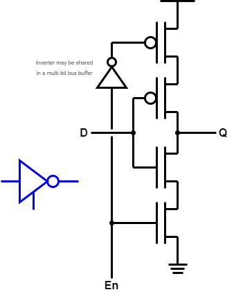
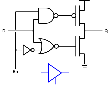
The ‘third’ signal state – high impedance (‘Z’) can be achieved by effectively disconnecting the logic driver from the power rails (left).
Buffers frequently need to drive large capacitive loads. To do this effectively it may be expedient to use larger (wider) transistors with only a single transistor ‘stacked;’ between the load and supply rail (right). The additional gate stage can provide amplification for driving a more powerful output stage.
If the concept of the transparent latch is not familiar there is a description in the lab. manual.

This structure demonstrates:
Omitting the ‘off’ transmission gates:
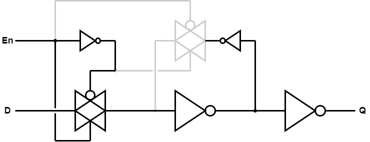
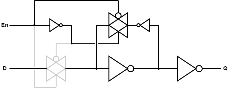
When enabled the input flows freely through the two inverters. The feedback is gated ‘off’.
When disabled the input is disconnected and a feedback path is used to retain the value. Feedback could be taken from ‘Q’ but, typically, a separate inverter is used so that any ‘noise’ (‘interference’) on the output network will not risk flipping the state. The feedback inverter may be made ‘minimum size’ because it never switches a node; it is simply there to retain charge.

If the feedback inverter is sufficiently weak (maybe made weaker by having lengthened transistor gates) a transmission gate may be removed.
Now, when switching the latch the input and feedback will drive in
opposing directions. As long as the input drive can switch the
‘middle’ inverter the feedback will soon
‘surrender’ and agree.
Just to demonstrate: a latch can be made reasonably efficiently with a (very) complex gate and a couple of inverters:

Note that this has also been arranged to drive the output from an inverter, which gives the best output drive for its transistor sizes.
This is still bigger (14 transistors vs. 12 or 10) and liable to be slower than the transmission gate/weak feedback design.
[More efficient latch structures are possible: space precludes …]
Up to CMOS index.
Back to CMOS gates.
Forwards to power consumption.