Energy = work done.
Power = work done per unit time
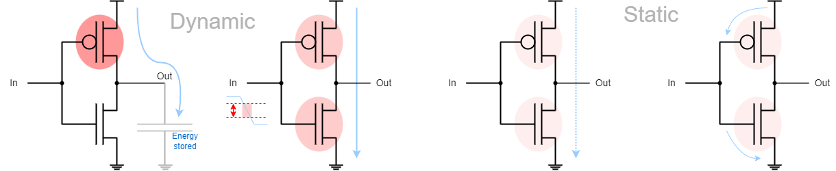
Energy stored = ½ C.V2
The dominant dissipation in active (switching) logic is the dynamic dissipation due to charging/ discharging load capacitance. This depends on the network load, the square of the supply voltage and the amount of activity.
The other dynamic component depends on the supply voltage, the transistor thresholds and the input edge speed.
Static (leakage) currents depend on the supply voltage and (for sub-threshold leakage) the transistor thresholds.
[‘α’ is the ‘activity factor’, representing the probability of a signal switching on a given clock edge.]
Dynamic dissipation is that which is caused by switching gates. It is therefore proportional to the clock frequency; at double the frequency gates switch twice as often so power is doubled. It is also related to the activity in the circuit: not every gate will switch on every cycle (except for the clock drivers) and, sometimes, logic blocks can be idle for long periods.
Dynamic dissipation in CMOS circuits is made up from two components: the first component is related to the load capacitance of a network. To switch a node to ‘high’ it is connected – via a pull-up tree – to the power supply and charge flows from there into the net (wires and transistors) until the voltage equalises.
This charge is defined by: Q = C.V
When the node discharges via the pull-down tree the charge flows to ground. The effect of the cycle is to move charge Q through the potential between the rails V, so the energy required/dissipated per cycle is: E = Q.V = C.V2.
This term does not depend on edge speeds, etc. Note, particularly, that this is proportional to the square of the voltage: halving the supply voltage will reduce the energy dissipation by a factor of four.
In more detail, this assumes a rail-to-rail swing of the signal. In some cases this change can be reduced, saving energy, but other problems may ensue.
The other dynamic dissipation comes from ‘short circuit’ or ‘crowbar’ current which results from both the pull-up and pull-down trees conducting (to some extent) as one turns off and the other turns on. This is difficult to quantify in general as it depends on a number of factors, including transistor widths and which transistors are switching. However there are two ‘simple’ ways to reduce this:
Improving power efficiency is a win-win strategy: improved battery life and fewer cooling problems. One thing a designer can do at RTL is to limit switching activity, particularly on ‘large’ buses (such as those connecting to memories which are physically large and therefore have significant parasitic capacitance).
Sometimes this is as simple as adding an ‘enable’ signal to registers to stop them switching when a component is not in use.
Static power dissipation happens continuously, regardless of switching activity. Historically it has been close to zero and therefore negligible except in very low power systems which are intended to do very little activity over very long periods using tiny batteries. However this source of inefficiency is increasing with technology advances.
Static dissipation is basically charge leakage through paths where charge is not supposed to go.
Subthreshold leakage is current through a transistor which is ‘turned off’. Transistors are not switches and will conduct to some extent at all times. A small current therefore flows through a gate even when it is not switching.
Subthreshold leakage can be reduced by having a high transistor threshold. However this slows down the gate switching speed by slowing ‘turn on’ and possibly also decreasing the ‘on’ transconductance. It is gradually becoming a more significant component in the overall power budget as the transistor threshold is forced down by the need to reduce the overall supply voltage.
Gate leakage is the leakage of charge from the transistor's gate to the silicon channel. Electrons go through the thin insulating (‘oxide’†) layer by quantum tunnelling; this effect increases exponentially with distance and so is an increasing problem as geometries shrink: the insulator thickness diminishes as well as the ‘horizontal’ dimensions.
Static power dissipation is still relatively small for most logic circuits but can account for a significant proportion of the power in memories, which have many transistors in a small space, most of which switch very infrequently.
Static dissipation in logic can be reduced by power gating: placing a high threshold transistor in series with the power supply which is switched ‘off’ when a set of gates is not in use. See later notes.
†Not usually SiO2 any more.
Up/back to power index.
Forwards to transistor thresholds.