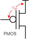
A CMOS transistor may be regarded as a switch. (For digital purposes.)
The threshold of a transistor is the gate voltage where it switches from ‘off’ to ‘on’.
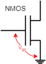
A CMOS transistor may be regarded as a switch. (For digital purposes.)
The threshold of a transistor is the gate voltage where it switches from ‘off’ to ‘on’.
Note: the transistor threshold is not the same as the gate threshold!
(i.e. where a logic element differentiates a logic ‘0’ and ‘1’.)
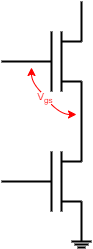
Different thresholds can be used to control energy flow.
Inverter response to a (slow – for clarity) input edge:
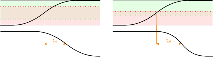
With low threshold transistors (left) the nMOS pull-down (green) switches ‘on’ earlier so the output edge starts sooner. The pMOS pull-up (red) switches ‘off’ later so there is a significant time when they're both ‘on’ allowing ‘short circuit’ current to flow between the power rails. This wastes energy. Fast but power-hungry.
With high threshold transistors (right) the nMOS pull-down switches ‘on’ later so the output edge is delayed. The pMOS pull-up switches ‘off’ earlier so there is little (or possibly no) time when they're both ‘on’, minimising ‘short circuit’ current. Low power but slow.
CMOS inputs should always be held at a logic level. If an input is not connected (“floating”) it has a (very) high impedance and may adopt just about any voltage. If it floats to somewhere between the logic levels then both the transistor stacks may turn ‘on’ (to some degree) and current ‘crowbars’ between the rails. This can be a significant power waste.
As long as the inputs are defined logic levels this is avoided and only the much smaller subthreshold leakage flows.
The threshold of a FET depends on the dopant concentrations in the channel and ‘diffusion’ implant regions. These are set by how many impurity atoms are embedded in the silicon substrate. This is a statistical process as atoms impact the surface.
For a given mean doping concentration, as transistor areas decrease the number of atoms decreases. This means the difference of a few atoms more significant overall.
The result is that the manufactured threshold voltages vary over an increasingly wide range as Moore's Law goes forwards.
Also called “back-biasing”, this is a mechanism where the ‘bulk’ (at least locally) silicon voltage is altered to move the transistor thresholds.
This can be used dynamically to influence the transistors' behaviour; it can also help counter threshold variations due to manufacturing variations (see later).
There is, of course, an added cost, especially in generating and distributing extra bias supplies. It is reported that the benefits are diminishing with shrinking feature size.
A silicon foundry may offer a range of transistor thresholds, some subset of which may be available on a single SoC. E.g.
These may be selected as appropriate in a design.
Example: use high-speed gates on the critical path and low-power gates away from there.
Low-leakage devices can also be used to power-gate high-speed logic.
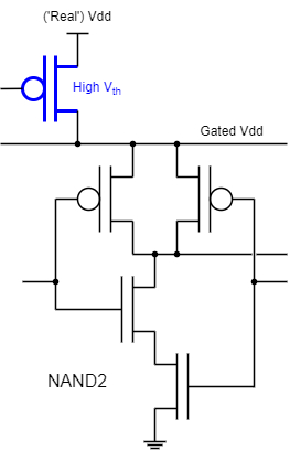
Power gating involves the creation of a separate, local supply rail for a gate of, more probably, a block of gates. This is supplied from the ‘real’ supply via a (large) pass transistor.
When active the pass transistor conducts and the gate will switch with (close to) the properties of the logic transistors. (There will be a slight penalty due to the additional channel impedance.)
When the logic is inactive the power can be cut off (the pass transistor is high-threshold so its leakage is small) and the remaining charge will leak to ground, after which leakage is minimised. Of course the gated ‘supply’ will be highly capacitive (much metal wiring) which means that when it's turned on it will take a significant time to be restored to operating voltage; thus power gating needs to be managed over time.
This figure shows a pMOS power gate: in practice, if a single transistor
is used, it is more likely to be an nMOS device because it can be
smaller for the same transconductance. It is even possible to gate
both supply rails to choke leakage even further.
Do not confuse the transistor threshold with a logic gate's threshold. The gate threshold is the input voltage where the whole gate will switch its output's logic state. This is typically around half the supply voltage: it will vary according to the gate's internal structure and may be (slightly) different on different gate inputs due to the position of connected transistors in the ‘stacks’.
Variation in gate threshold is a good reason to keep signal edges fast – to minimise differences in when they are perceived to change.
Up to power index.
Back to power dissipation.
Forwards to power domains.