Extending the idea of power gating, different parts of a SoC may be powered from different voltages.
Slower regions can be run off reduced voltage rails.
On a SoC it may be appropriate to run different parts of the device under different conditions, such as different supply voltages.
Lower supply voltages typically mean slower switching speeds but that may be acceptable for some units on a SoC. Lower voltages will also reduce power consumption.
A problem encountered with different supply voltages is the interpretation of signals at domain boundaries. (This is similar to the problem of crossing boundaries between differently clocked domains, but can be resolved reliably.)
A clock distribution network is a high-load net (it fans out to many places) which switches frequently (twice per clock cycle). It therefore can be a major contributor to power dissipation.
It is now quite common to employ clock-gating to blocks which are idle, even if the rest of the logic is not switching. CAD tools will support this. Note – DIY gating is dangerous: clock gating must not introduce glitches when turned on and off, nor impose arbitrary clock skew.
The power can remain on so register/memory state is retained.
It is not uncommon for an embedded processor core to go into a gated ‘sleep’ mode whilst waiting for an interrupt; the active interrupt signal restarts the clock so processing resumes.
A place where leakage power is dominant is in memory. SRAM does not do much logic switching (compared to registers or logic) but does have a high transistor density. If it is not being used for a period it is possible to reduce the supply voltage: the memory is able to retail its state although it cannot be accessed until the full supply is restored. Whilst ‘asleep’ the leakage power is reduced. This may be very significant in extremely low power (typically embedded) applications.
The ultimate power-saving option is to switch off. “Dark Silicon” is a term coined to refer to parts of a system which are present but may be unpowered.
By switching off domains of an SoC which are not in use at a particular time all the dissipation can be avoided, including leakage currents.
This may be necessary – rather than just desirable – in some devices to stop the power dissipation exceeding that which keeps the temperature within operating limits.
There are some disadvantages to this strategy: from the logic point of
view it must be ensured that signals which emerge from a powered-down
domain are clamped to harmless values. More importantly, when
switched off, all the register and memory (RAM) state is lost so there
may be considerable work in restoring context when switched on
again.
(Future, non-volatile storage may address this, one
day.)
This technology may be expected proliferate as many-core processors become common and the need to maximise processor utilisation is no longer a major consideration.
ARM has a mechanism called ‘big.LITTLE™’ which
employs two (sets of) code-compatible ARM cores: a high-performance
(high-power) one and a low-performance (low-power) device. The
high-performance core is turned on only when processing demand merits
it and execution is then migrated to it.
More recently there might also be ‘middle (sized)’
processors between the extremes, offering even more power/performance
flexibility.
Note that, to achieve high performance, various mechanisms such as speculation may be employed which use energy for acceleration rather than evaluating the actual problem. For example, deeper pipelines will process more items which are, sometimes flushed and discarded.
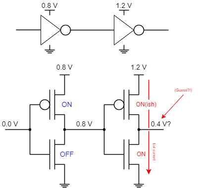
Running from different supplies can cause problems:
Static power is dissipated … output ‘level’ may not fully switch next gate …
Normally ‘ground’ is a common reference so, when crossing between domains with different supply rails it is the definition of ‘high’ which will vary. The primary problem occurs when an input ‘high’ (say 0.8 V) may be below the threshold of a pMOS transistor in a higher voltage domain. In this case the pMOS transistor will not turn ‘off’. Even if the gate reads this signal as a ‘high’ there will be a continuous current drawn from the supply, dissipating power in the interface transistors.
In the case on depicted here the output (‘low’) might be high enough to turn on the next nMOS transistor(s) partially too, propagating the problem further.
What is needed is a reliable way of achieving the output levels in the new supply domain.
Need to transform a ‘high’ when moving to a different supply domain. Here's one way:
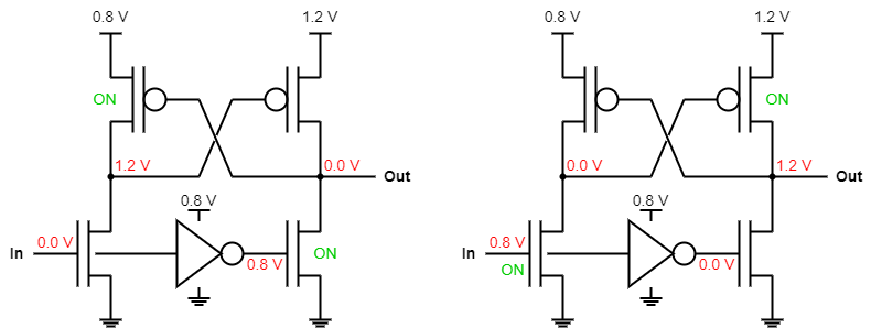
In this design a ‘low’ is always 0.0 V, so that needs no translation.
There are many and varied level shifter designs. In this example the input pulls one side of the differential amplifier low whilst not affecting the other. This causes one of the pMOS transistors to turn ‘on’ whereas the other is not sure. The ‘turned on’ pFET has nothing to oppose it and will pull up the gate of the other, turning it ‘off’. This prevents further current flow through the nFETs whilst the output (or its inverse) is clamped to the higher voltage supply.
This is not the fastest level shifter but it illustrates how the job can be done.
There are many other level shifter designs. You might like to discover and sketch some.
If you're a microcontroller hobbyist (or sinilar) you might find a similar requirement at the circuit board level — typically between 5.0 V and 3.3 V.
There are circuits – including integrated circuits† ‐ to help with this.
†Supplier example: not specifically endorsed.
Dynamic Voltage/Frequency Scaling
If there is not much work to do:
When there is a high work demand:
A similar approach may be employed if the power dissipation (i.e. temperature) gets too high.
DVFS (Dynamic Voltage and Frequency Scaling) is, perhaps, currently falling out of favour because supply voltages are reducing such that there is not much ‘headroom’ for scaling. However the principle works like this:
So, if it is allowable to run more slowly:
These values are not exact but a reasonable ‘rule-of-thumb’.
This can be applied dynamically if the workload can be predicted, slowing down when there's no rush and speeding up when the demand is high.
Note: reduce frequency before reducing supply voltage. Increase supply voltage before increasing frequency. (If you want it to work correctly!)
Power management can be vital in SoCs, especially now there are extreme levels of integration. A modern SoC may be capable of dissipating enough power to overheat and destroy itself; thus it needs to keep domains not in use running at reduced power or turned off. This is likely to involve quite complex support from software (operating system), possibly with feedback from on-chip temperature sensors.
There may be more facilities available than mentioned previously in this lecture: for example it is possible to reduce the supply voltage to SRAM (thus limiting leakage) such that the RAM cannot be used but still retains its data: good for long-duration ‘sleeps’. Similarly, many processors now support a WFI (‘Wait For Interrupt’) instruction which gates-off the processor clock (mostly) to minimise activity (whirling around waiting for something to happen) when not in use.
If you haven't come across it, you might also be interested to check out big.LITTLE and its successors.
These can combine with clock and supply voltage scaling, and temperature monitoring, and battery charge state, to deliver (in principle!) adequate performance with economy.
Up to power index.
Back to CMOS gates.
Forwards to ASIC production.