Without delving deeply into the topic, a significant constraint on a chip is the number of external contacts it can have. These may be referred to (often interchangeably) as “pads” (the contact position on the silicon) or “pins” (the metal contact outside the package).
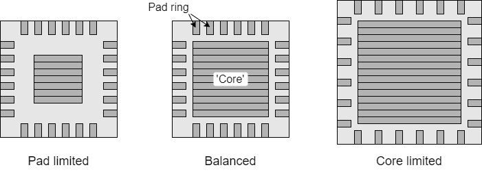
A ‘traditional’ chip will have a ‘pad ring’ around its periphery. Each pad occupies a significant space because it has to be large enough for a bonding machine to attach a wire. It also contains amplifiers to drive the much larger off-chip loads and significant electrical protection. Pads will be linked with ‘large’ tracks to aid power supply distribution.
A (logically) very small device may be ‘pad limited’ in that, once the pads are placed and spaced, the central ‘core’ area is not filled.
Because silicon costs – so smaller chips are cheaper – there may be a desire to reduce the ‘pin count’. This is another trade-off for the chip designer to consider.
Example: many microcontroller chips have numerous peripheral interface devices on board. It is probable that not all of these are wanted by any specific user. It is common practice to multiplex I/O connections so that particular functions can appear on particular pins and the user can select his own variety. This also means the chip is less specific to particular applications so fewer different types of devices have to be designed, built and tested.
A current example of this may be observed with the Raspberry Pi's expansion port.
Note: the chip core scales with the square of the linear dimensions, the pad wing scales linearly.
A modern trend is away from a peripheral pad ring to ‘flip-chip’ mounting. This leads the external contacts to ‘microbumps’ which protrude from the passivation over the top of the circuit, i.e. above the highest metal wiring layer. The chip is mounted ‘upside down’ in the package, the grid of bumps connecting with contacts on the package.
This gives a couple of advantages:
A major reason that these can be important is supplying power where more wires are needed to satisfy the increasing current demands and the inductance of long (thin) bond wires exacerbates electrical noise problems.
[Don't confuse this with the BGA mounting of packages to PCBs, which is geometrically similar but on a larger scale.]
Packages also come in standard sizes. This may also constrain the size of the die, since it must fit inside.
Typical IC packages are built to mount onto a planar Printed Circuit Board (PCB), with contacts on (or around) the package ‘bottom’. Package-on-Package allows a package to be mounted in a stack on the ‘back’ of another package. This saves PCB space – useful in applications such as mobile 'phones – and reduces power dissipation because there is less capacitive load on the chip interconnection. However it may be inappropriate for higher power systems since it increases the (physical) power density, exacerbating any cooling problems
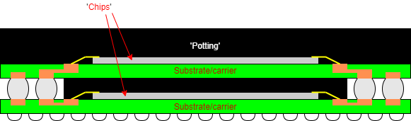
A ‘familiar’ example is probably the Raspberry Pi which has its SDRAM mounted on the back of the main SoC.
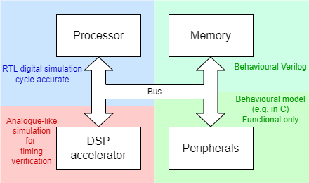
It is infeasible to simulate a whole SoC very precisely in one run.
Instead, use different (precision/cost trade-off) simulators for different blocks. Example:
Each new block can be verified in an environment which has ‘appropriate’ accuracy.
In some cases this will be as high as a
Transaction
Level Model (TLM).
There are various analogue circuit simulators (e.g. HSPICE, Spectre) which tend to be known, generically as ‘SPICE’ (Simulation Program with Integrated Circuit Emphasis) after the original tool gained wide acceptance.
SPICE takes, as input, a component netlist, an input stimulus file and detailed models of the components' characteristics. It simulates circuit activity solving differential equations, giving an accurate model of the circuit's behaviour when fabricated. Of course, this takes significant processing time so SPICE simulations tend to be limited to small circuits and limited time runs.
A typical application of SPICE would be to characterise standard cells, producing simplified (if less accurate) models to be used in larger analogue simulations. For example, a NAND gate may be ‘Spiced’ to determine the propagation delay and output edge speeds into different loads when switched with each input (in each direction) with different input edge timings.
Feedback from this process will be used to ‘tune’ the performance of layout – for example to determine the transistor widths for different cells.
SPICE may not be needed by a high-level designer but it (or an equivalent) will be used somewhere in the design flow and it becomes necessary if designing analogue or other custom circuits.
Not every chip made will function in quite the same way due to variation in the manufacturing processes their transistor properties will vary. Because they are manufactured in different steps, the pMOS and nMOS transistors may differ from the ‘nominal’ properties in different ways.
The operating environment of chips will vary. The two greatest variables will be operating supply voltage and temperature. Lower voltages or higher temperatures will slow down switching.
These variations are normally classified as ‘PVT’ (Process, Voltage, Temperature) variations.
It is important that the chip works over a wide range of conditions. Thus, physical simulation will normally be carried out over a number of process ‘corners’, i.e. with different assumed transistor characteristics: {fast-fast, fast-slow, slow-fast, slow-slow, typical} processes are considered (the terms refer to p- and nMOS transistor speeds). Voltage variations of 10% may be tried. Temperature ranges vary according to application, from -40°C or 0°C at the bottom end to 85°C, 100°C or maybe 125°C at the high end. The device should function (at the target speed) over all these variations.
Note: this involves running a whole set of functionally identical simulations using a timing-accurate simulator/model.
The chip manufacturer may regard the internal layout of their standard cells as confidential. Layout will therefore not be available. Instead they supply a library of ‘phantom’ cells which show the sizes and possible connection points. These will be accompanied by simulation models characterised from the layout to allow development without revealing details.