Notes revised 2024.
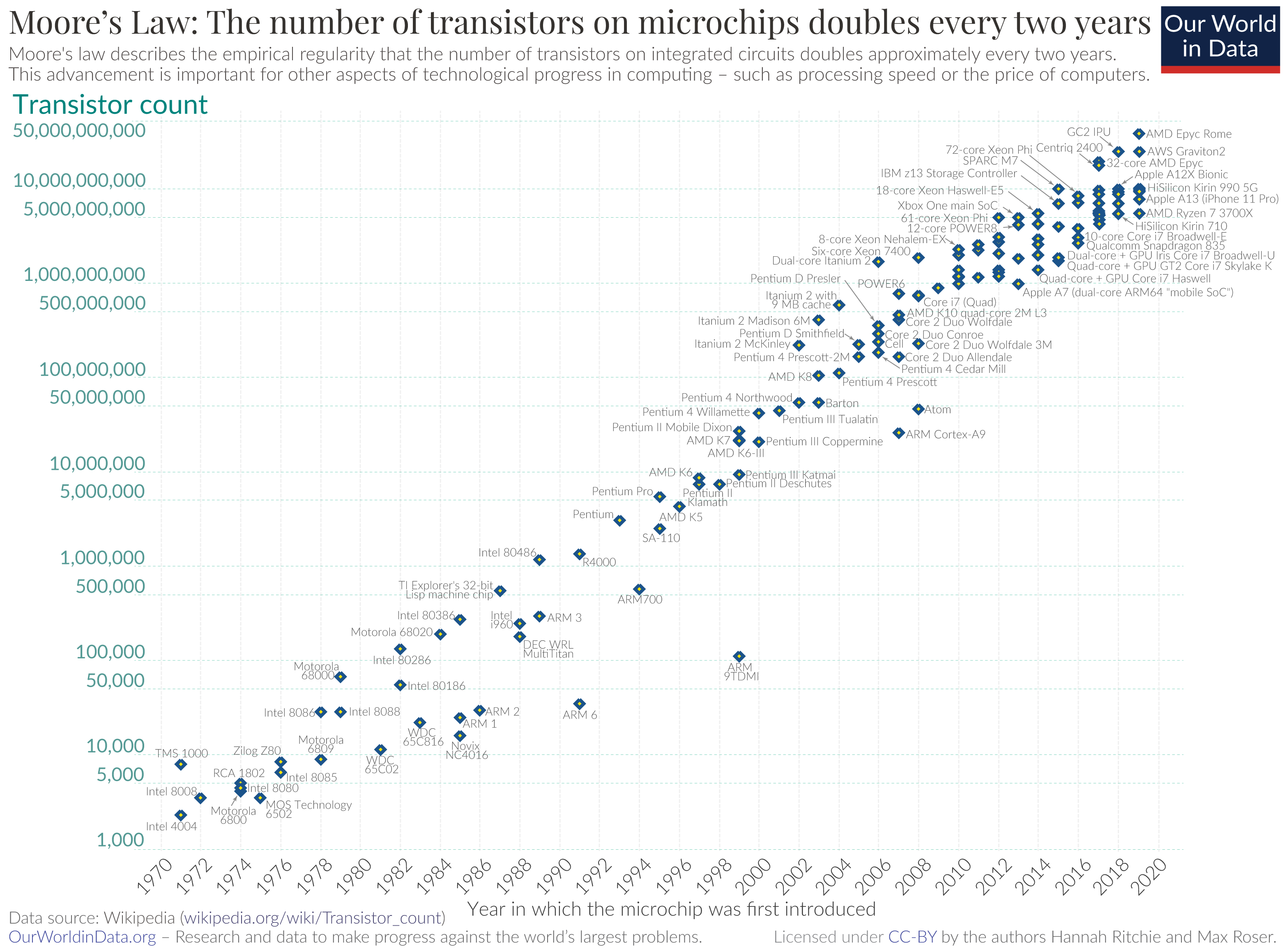
Note logarithmic scale.
Taken shamelessly from Wikipedia.
Alternatively, looking at the smallest available feature size:

Note logarithmic scale.
Red (2025) is speculative at time of writing.
Data from Wikipedia: plotted locally.
Producing devices is all very well but they need to do something useful. There is an increasing ‘design gap’ between what can be made and how it is designed. Whilst CAD tools and synthesis make designers more productive much of the transistor budget is devoted to repetitive structures such as memories. The expanding number of ‘cores’ on processors is an obvious symptom.
Within an order of magnitude, all atoms are about the same size which is one angstrom (Å) or 10-10 m (or 0.1 nm) in radius. A 3 nm gate length is therefore about 15 atomic diameters across. The dielectric thickness is already much less, perhaps ~1 nm so only a few atoms thick.
Clearly a single atom is a hard limit to anything physical. However, at least using CMOS technology, the material must also retain its ‘bulk’ properties.
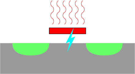
Chips are made using photolithography and the feature size (3 nm [2024]) is already much smaller than the wavelength of the light used (193 nm) which is towards the middle of the ultraviolet spectrum. Using shorter wavelength light is increasingly difficult as optics is hard – think about trying to make lenses for X-rays!
It is possible to achieve higher resolutions using electron or ion beams; compare what is visible under a light and an electron microscope. However a beam needs to be scanned whereas optical exposure can print over large areas.
Therefore making structures photolithographically is akin to printing whereas using direct beams is more like handwriting. It is clear which technique is amenable for mass production!
As chips get smaller they get harder to make. The machinery needs to be more precise (so it gets more expensive) and there are more manufacturing steps (which increase the cost). The resulting products still need to be cheap; if the cost rises more than the benefit then shrinking becomes uneconomic.
For many years ‘popular’ logic devices used a 5 V supply. Two big problems as devices have shrunk:
To combat these, core† supply voltages have been gradually reduced, now to below 1 V, a trend which must continue. This makes the transistor ‘on’ and ‘off’ states closer together (probably increasing ‘off’ leakage) and reduces the noise margins available so that electromagnetic interference or radiation can produce upsets more easily.
At PCB level, where different parts are assembled (and electromagnetic interference will be greater due to the larger ‘aerials’ (tracks)) the voltage reduction has been more conservative, having largely reduced only to 3.3 V (a.k.a. ‘3V3’). Of course this necessitates level shifting at the chip's pads.
†At the logic core of the device. Pad voltages interfacing with the PCB are higher to provide better electrical noise immunity and backward compatibility with pre-existing devices.
‘K’ is the ‘dielectric constant’, more
properly called the ‘relative permittivity’
(εr). It is a measure of the electric field strength in the
dielectric. Replacing SiO2 as a dielectric allows a
thicker separator (less leakage) yet greater capacitance (which is
what switches the FET).
Materials containing elements such as hafnium or zirconium are typical.
For rough reference, window glass (SiO2) has a breakdown dielectric strength around 10 MV/m (10 V/μm).
Moore's Law is now reaching its limits. Really!
For many years the International Technology Roadmap for Semiconductors (ITRS) described plans, expectations amd aspirations for the future development of the technololgy. This is now superseded by the International Roadmap for Devices and Systems (IRDS). For future news, watch that space.
Here's another video – [2024] (25 mins.). Hopefully this is now all revision!
That's all folks!